VA charakteristics of LED - Measurement of Planck constant
Physical Background
Electrons in atoms obey Pauli excluding principle – there are no two electrons with same sets of quantum numbers values. So the elcetrons sit on energy levels from the lowest one. At zero temperature (0 K), there is no energy level from the lowest one to the highest one, which would be not occupied.

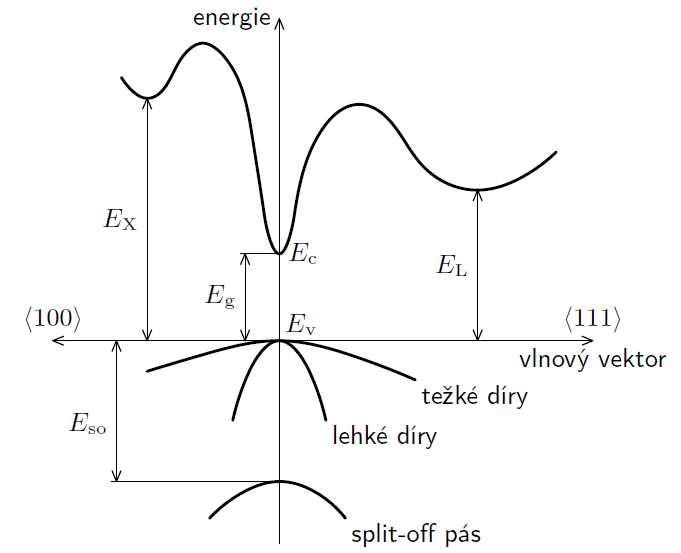
Fig 1.: Band structure of GaAs
In solids we observe remarkable effect. Energy levels of electrons are very close, so the electrons have nearly continuous spectrum of energy (which is result of too many electrons present in solid). However, there are intervals of energy, which none of the electron can have, these energies are forbidden. Dependence of electron energy on wavelength vector is called band structure, since the allowed/forbidden energies form bands.
In semiconductors configuration, the difference between highest ocuppied energy Ev and first unocuppied energy Ec is called forbidden band, its height is defined as Eg = Ec – Ev. The highest occupied band at zero temeperature is called valence band and the lowest unoccupied band is called conduction band. In real semiconductors, at standard conditions (eg. non-zero temperature) some electrons difund from occupied band to unoccupied band because thermal effect. Band structure of a semiconductor can't be computed analytically, but can be computed using numerical methods. Example of numerically computed band structure of semiconductor of type III-V galium-arsenid is on picture 1.
In conduction band E ≥ Ec the elcetron can increase its energy (eg. in electric field) Ve vodivostním pásu E ≥ Ec může elektron libovolně zvyšovat svou energii (např. v elektrickém poli), because in its neighborhood there are enough unoccupied energy levels. On contrary, in valence band E ≤ Ev the electron is bounded, since the energy levels are occupied and it can't so easily jump into another level. Valence and conduction band are nearly connected in conductors, so due to thermal movement the electron can be released into conduction band and conduct electric current. In case of semiconductors it can be done by absorbtion of sufficient amount of energy, eg. by photon of energy E such that

where h is Planck constant, c is speed, ν frequency and λ is wavelength of light in given material (we can assume vacuum). The semicondutors and insulators differ by value of forbidden band. (for insultators Eg 5 eV). Different semiconductors diifer by value of Eg.
Used LEDs are made of Ga-As semiconductor, which has direct transition. This means that absorbtion/emission of photon is sufficient to transfer energy to/from electron without impuls loss/gain. (In band structure on fig. 1 it means, that minimum energy Ec is directly above maximum Ev.) LED (light-emitting diode) uses opposite jump from conduction band to valence band (this phenomenon is called spontaneous emission), and the photon of energy E ≥ Eg is emitted. Firstly it is needed to transfer sufficient energy to electron to jump into conduction band. The mentioned process of thermal oscillation is insufficient, so the work W can be done by electric field with voltage U
![]()
where e is absolute charge of electron. Then we obtain inequality
![]()
Emitted wavelength λ and voltage U can be measured (in worst case it can be found in catalogue of components). The LED can glow only if certain minimal voltage is present, its existency is explained in eq. 1. In idealized state we can assume that voltage U can be measured in the moment, when the LED start glowing, and then the inequality becomes equality. Don't forget to discuss these asumptions in discussion.
